Diffusion Bonded Microfluidic Chips
Adhesive-free acrylic (PMMA) and PEI microfluidic chips and manifolds. Molecular-level bonding keeps channels clean, optically clear, and leak-free - from 2-layer research chips to 5-layer instrument manifolds.
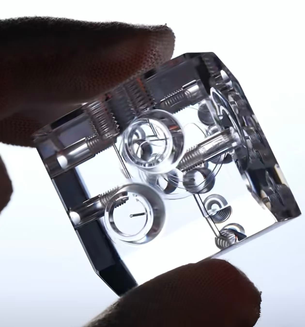
Two Materials, One Bonding Process
Every chip is machined from solid plate and joined by thermal diffusion bonding - no adhesives, no solvents, no contamination inside the microchannels.
Acrylic (PMMA) Chips
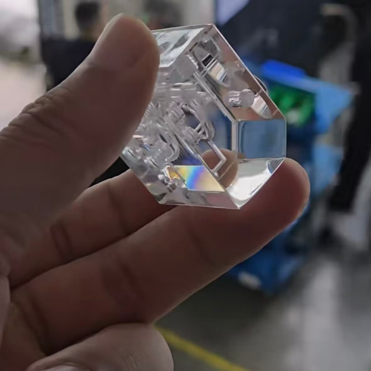
Optically clear, cost-effective, ideal for diagnostics
- ✓92% light transmission for optical detection and visual flow inspection
- ✓Low autofluorescence, biocompatible grades available
- ✓Continuous use up to 80°C
- ✓Best cost-performance for single-use and prototype devices
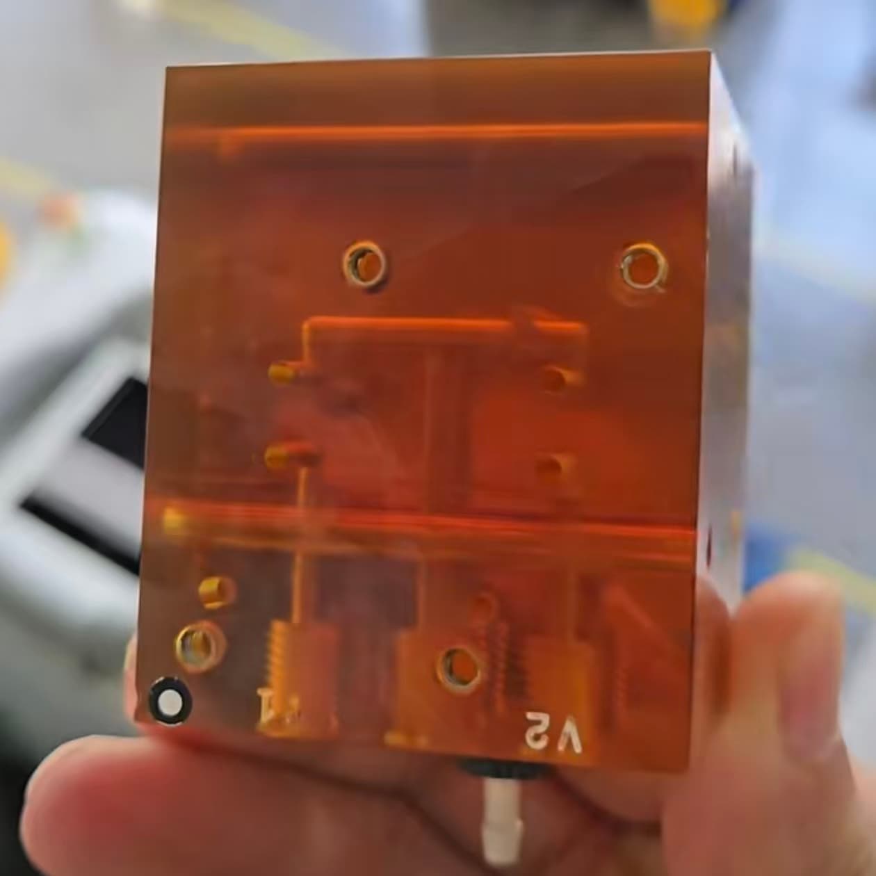
PEI (Ultem) Chips
High-temperature, autoclavable, chemically resistant
- ✓Glass transition temperature 217°C - survives repeated 134°C autoclaving
- ✓Excellent resistance to solvents, acids, and bases
- ✓High mechanical strength for reusable instrument manifolds
- ✓Amber translucent body, USP Class VI grades available
How Diffusion Bonding Works
Diffusion bonding joins polymer layers at the molecular level under controlled heat and pressure - creating smooth internal channels impossible to produce with adhesives or conventional machining.
Precision CNC Machining
Microchannels, chambers, and port threads are milled into each layer with ±0.05 mm tolerance. Channel widths from 100 μm with smooth, burr-free walls.
Surface Preparation
Bonding faces are polished to optical flatness and cleaned in a controlled environment to remove particles and contaminants.
Alignment & Stacking
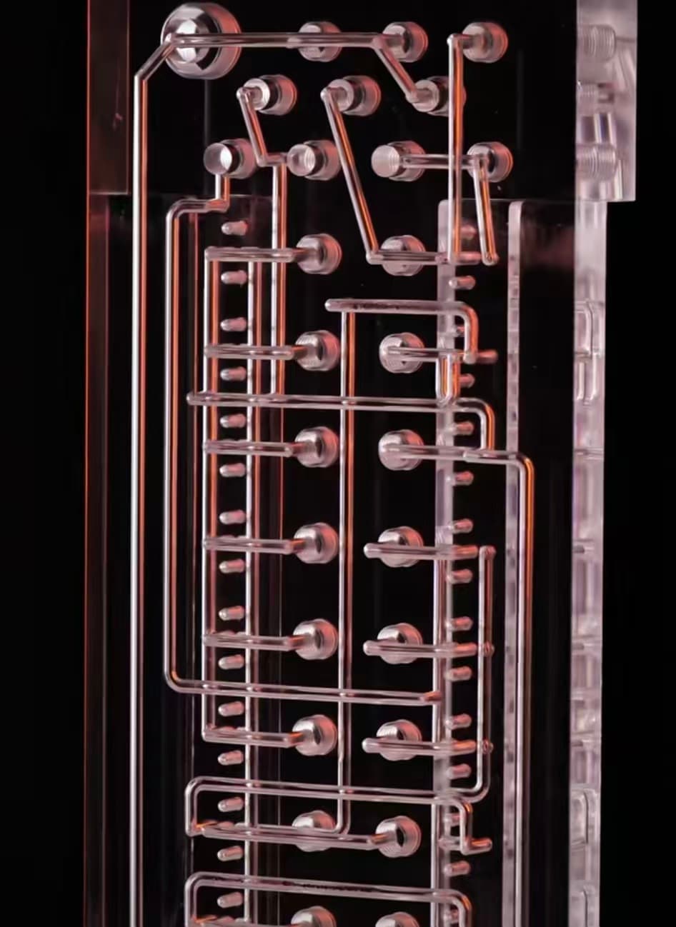
Layers are aligned with precision fixtures and stacked - from simple 2-layer chips to complex 5-layer manifolds with crossing 3D channel routes.
Diffusion Bonding
Under controlled temperature and uniform pressure, the polymer surfaces fuse at molecular level. No adhesives, no solvents, no foreign material in the channel.
Annealing & QC
Bonded parts are annealed to relieve stress, then leak-tested, dimensionally verified, and optically inspected before shipment.
Acrylic vs PEI at a Glance
| Property | Acrylic (PMMA) | PEI (Ultem) |
|---|---|---|
| Optical clarity | 92% transmission, water-clear | Amber translucent |
| Max continuous temperature | ~80°C | ~170°C (Tg 217°C) |
| Autoclave sterilization | Not recommended | Yes, repeated cycles at 134°C |
| Chemical resistance | Good with aqueous solutions; limited solvent resistance | Excellent - most solvents, acids, bases |
| Autofluorescence | Low | Moderate (amber tint) |
| Typical use | Diagnostic cartridges, POCT, research chips | Reusable instrument manifolds, analyzers |
| Relative cost | $ | $$$ |
Recent Production
Technical Specifications
Applications
Point-of-Care Diagnostics
Cartridges for immunoassays, nucleic acid testing, and blood analysis
IVD Instrument Manifolds
Consolidated fluid paths replacing tubing in analyzers and sequencers
Cell Culture & Organ-on-Chip
Perfusion channels and culture chambers with optical access
Droplet Microfluidics
Flow-focusing junctions and droplet generation networks
Analytical Instruments
Sample handling for chromatography, spectroscopy, and titration
Research Prototyping
Fast-turnaround custom chips for academic and industrial R&D
Frequently Asked Questions
What is diffusion bonding and why is it better than adhesive bonding?
Diffusion bonding fuses polymer layers together under controlled temperature and pressure without any adhesive. The bond line contains no foreign material, so microchannels stay free of glue overflow, air bubbles, and extractables that could contaminate samples or block 100 μm channels. Bond strength approaches that of the parent material, and acrylic parts remain optically clear across the joint.
Should I choose acrylic or PEI for my microfluidic chip?
Choose acrylic (PMMA) when you need optical clarity for fluorescence or visual detection, low autofluorescence, and the lowest unit cost - typical for diagnostic cartridges and research chips operating below 80°C. Choose PEI when the device must survive autoclaving, contact aggressive solvents, or operate at elevated temperatures - typical for reusable instrument manifolds and analyzers.
How many layers can you diffusion bond?
We routinely produce 2-5 layer stacks. Two-layer chips suit most channel-over-cover designs, while 3-5 layer manifolds allow crossing channel routes, integrated chambers, and dense port arrays that would be impossible to machine from a single block.
What fluidic connections do you support?
Standard 1/4-28 UNF flat-bottom ports for conventional microfluidic fittings, M6 threads, and custom port geometries. Ports are machined directly into the chip body, so no glued connectors are required.
What is the typical lead time and MOQ?
Prototypes ship in 2-3 weeks from approved drawings. There is no tooling cost because chips are CNC-machined rather than molded, so MOQ starts at 10 pieces - practical for R&D and pilot production. Volume orders receive scaled pricing.
What files do you need for a quotation?
A 3D CAD file (STEP preferred) plus a 2D drawing with critical dimensions, channel cross-sections, layer breakdown, and port specifications. If you only have a concept sketch, our engineers can help complete the design for manufacturability.
Ready to Build Your Microfluidic Device?
Send us your CAD file or concept sketch. Prototypes in 2-3 weeks, MOQ from 10 pieces, no tooling cost.